Canon’s Nanoimprint Lithography: A Potential EUV Challenger?
Introduction
The semiconductor industry is in a constant state of evolution, with lithography playing a pivotal role in pushing the boundaries of what’s possible. As transistors shrink and chip complexity increases, the demand for more precise and cost-effective lithography techniques intensifies. While Extreme Ultraviolet (EUV) lithography currently reigns supreme, Canon is making waves with its Nanoimprint Lithography (NIL) technology, presenting a potential challenger to the status quo.
What is Nanoimprint Lithography (NIL)?
Unlike traditional photolithography, which uses light to etch patterns onto silicon wafers, NIL employs a more direct approach. Imagine using a stamp to imprint a design – that’s essentially how NIL works. A pre-fabricated template, or “mold,” containing the desired circuit pattern is pressed directly onto a layer of resist on the wafer. This direct contact method eliminates the need for complex and expensive optical systems, potentially offering a more cost-effective solution for high-resolution patterning.
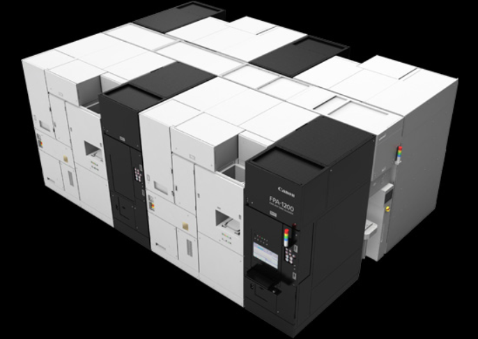
Canon’s FPA-1200NZ2C: A Closer Look
Canon’s latest NIL system, the FPA-1200NZ2C, boasts impressive capabilities. With a minimum linewidth of 14nm, it can produce chips comparable to those made using ASML’s leading EUV scanners. This achievement positions NIL as a viable alternative for manufacturing chips using 5nm process technology and potentially even smaller nodes in the future.
Advantages of NIL
NIL offers several key advantages over traditional photolithography:
- High Resolution: NIL can achieve extremely fine resolutions, pushing the limits of miniaturization and enabling the creation of smaller, more powerful chips.
- Lower Cost: By eliminating the need for complex optics and high-energy light sources, NIL has the potential to significantly reduce manufacturing costs.
- 3D Patterning: NIL excels in creating three-dimensional structures, opening doors for new possibilities in chip design and functionality.
- Improved Pattern Fidelity: The direct contact method used in NIL ensures high fidelity pattern transfer, resulting in more precise and uniform features.
Challenges and Limitations of NIL
Despite its promise, NIL faces certain challenges that must be addressed before it can fully challenge EUV lithography:
- Defect Sensitivity: The direct contact nature of NIL makes it susceptible to defects caused by particles or contaminants. Maintaining pristine manufacturing environments is crucial for high yields.
- Throughput Limitations: Traditional NIL is a serial process, meaning patterns are imprinted one at a time. This limits its throughput compared to the parallel processing capabilities of photolithography.
- Mask Durability: The molds used in NIL can degrade over time, requiring frequent replacement and adding to manufacturing costs.

Applications Beyond Chip Manufacturing
While NIL’s potential in chip manufacturing is significant, its applications extend beyond the realm of CPUs and GPUs. The technology shows promise in areas such as:
- High-Density Data Storage: NIL could enable the creation of patterned media for hard disk drives, leading to significant increases in storage capacity.
- Advanced Photonics: The ability to create precise 3D structures makes NIL well-suited for manufacturing advanced photonic devices used in fiber optic communications and other applications.
- Biotechnology: NIL’s high resolution and ability to pattern various materials make it a valuable tool for creating biosensors and other microfluidic devices.
The Future of NIL and EUV Lithography
While EUV lithography remains the dominant force in advanced chip manufacturing, Canon’s advancements in NIL present a compelling alternative. It’s unlikely that NIL will completely replace EUV in the near future, but the two technologies could coexist and complement each other.
For example, NIL could be used for specific manufacturing steps where its unique advantages shine, such as creating certain 3D structures or high-resolution features. Additionally, NIL could play a crucial role in the development of next-generation EUV masks, further pushing the boundaries of lithography.
Conclusion
The semiconductor industry thrives on innovation, and Canon’s foray into NIL injects a healthy dose of competition into the lithography landscape. While challenges remain, the potential of NIL to disrupt the status quo and drive further advancements in chip manufacturing is undeniable. As both NIL and EUV technologies continue to evolve, the future of semiconductor manufacturing promises to be exciting, with both playing crucial roles in shaping the technological landscape of tomorrow.
High-Trust External URLs:
- IEEE Spectrum: https://spectrum.ieee.org/
- Semiconductor Engineering: https://semiengineering.com/
- Nature Nanotechnology: https://www.nature.com/nnano/


